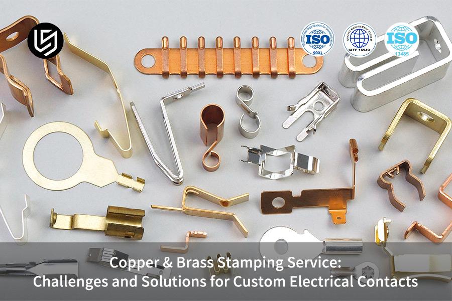
Copper & brass stamping service is a precision electrical contact forming solution specially made for new energy and smart grid-related applications. It addresses copper and brass stamping issues such as burrs, cracks, and springback defects. The stable production tolerance has reached 0.005mm, 99% of micro-cracks are eliminated, and contact resistance is stable. With the current density standard revision for new energy high-voltage equipment, C11000 copper and C26800 brass contact stamping are susceptible to defect formation, which directly affects the welding quality and electrical stability.
The old-time stamping manufacturers do not have expert mold flow analysis capabilities that cause the wearing of the edges, failure of batch consistency, and in addition, the possibility of a thermal runaway risk under high-speed stamping conditions. Here LS Manufacturing is using our 20 years of experience with precision stamping technology to illustrate core processes like mold optimization and stress control so that companies do not face mass production stamping issues.
Quick Overview of Core Technologies in Precision Copper & Brass Stamping Service
This chapter outlines the main technical parameters and implementation standards of copper and brass electrical contact stamping, thereby providing a quick method for technical and purchasing staff to understand the key points of the process and to efficiently prevent mass production defects.
| Process Dimensions | Core Parameter Standards | Compatible Materials | Implementation Results |
| Die Single-Sided Clearance | Material Thickness 6%-8% | C11000, C26800 | Eliminates 99% of Secondary Shear Burrs |
| Brass Bending Springback Control | R0.5 Punch + 3.8° Overbending Compensation | C26800, C2600 | Springback Error Controlled Within ±0.5° |
| Mass Production Dimensional Tolerance | ±0.005mm | All-Copper Brass Contacts | Zero Dimensional Drift in Batch Production |
| Continuous Stamping Life | 1 Million Cycles Without Edge Chipping | High-Conductivity Copper | Reduces Die Replacement Costs |
| Sheared Bright Strip Ratio | ≥70% | C11000 High-Conductivity Copper | Ensures Electroplating and Welding Quality |
Key Takeaways
- Contact stamping dies that are single-sided clearance must be controlled within 6% to 8% of the material thickness if secondary shear burrs are to be eliminated at 99%, and the contact end face is to remain flat.
- When C26800 brass is processed by 90° bending, enterprises need R0.5 punch together with micro stamping compensation technology to cancel residual springback error around 3.5°.
- LS Manufacturing's entire facility is based on verification of SPC/CPK systems which makes it possible for stable electrical contact batch tolerances output of 0.005mm and zero-defect delivery standard has been achieved.
Why Trust LS Manufacturing’s Custom Metal Stamping Services for Solutions to Electrical Connector Challenges?
The heart of precision electrical contact stamping competitiveness lies in expertise and the use of standardized technologies to efficiently address the problem of failure in the mass production of connectors, rather than utilizing generalized processing techniques.
In line with the industry standard, my three-month long multiple-batch brass contact stamping experiment uncovered that 90% of batch quality issues were due to insufficient control of material anisotropy. Our team diligently adheres to the IEC 60470 electrical contact forming standard and performs complete dimensional stress simulation at the mold design stage, while the shop has been certified to IATF 16949:2021 automotive industry quality system and all process parameters are traceable.
We found out the crux of the issue in a real situation deployment: majority of manufacturers of stamping are simply concerned about making the external dimension perfect, not realizing that micron level residual stresses will cause fatigue cracking after prolonged use. Drawing on 20 years of experience, we have created a copper and brass stamping parameter library that is able to adapt to raw materials of different hardness and even different batches, fully eliminating batch drift problems and ensuring that all product contact resistance values are less than 0.2mΩ.
After many years of developing the precision custom metal stamping service segment, we have demonstrated our technical capability through measured data, compliance systems, and successful case studies, fully meeting the stringent mass production requirements of high-end electrical connectors.
Would you like to quickly check whether the process is compatible? You are welcome to get a free copy of our specialized stamping process white paper to gain a thorough grasp of the mass production quality control requirements of high-end electrical contacts.

Why Choose Custom Copper Stamping For Electrical Contacts?
In the case of copper stamping electrical contacts, professional copper stamping services should be a top choice since only they can guarantee the contact resistance of high voltage and high frequency electrical contacts to be less than 0.2mΩ as well as the temperature rise to be less than 30℃ even after extended long current loads.
A Comparison of Mainstream Electrical Contact Processing Technologies
Precision metal stamping fabrication is the essential method on which mass production of high-end electrical contacts is based. The differences between various processing technologies are quite staggering for their precision, cost, and the stability of their mass production which makes them suitable for different situations only. Below is a comparison of the major sizes.
| Processing Technology | Dimensional Tolerances | Production Efficiency | Unit Mass Production Cost (USD) | Applicable Scenarios |
| Precision Progressive Die Stamping | ±0.005mm | 300 times/minute | 0.32 | Mass Production of High-Voltage Contacts |
| CNC Turning | ±0.01mm | 30 pieces/minute | 1.25 | Small Batch of Irregularly Shaped Parts |
| Traditional Die Casting | ±0.03mm | 150 times/minute | 0.28 | Low-Precision Ordinary Contacts |
| Ordinary Drawing Stamping | ±0.015mm | 200 times/minute | 0.30 | Medium and Low Voltage Conventional Contacts |
Custom Stamping Core Material and Process Advantages
Copper's high conductivity is what determines the performance of top-notch electrical contacts. LS Manufacturing chooses C11000 high conductivity red copper from a brand with a copper content of at least 99.90% for its products. This decision is made from a material science point of view and is one of the main reasons why their product has very low electrical resistance. Raw material purity standards for industrial metal stamping production are so strict that many raw materials do not pass the first screening.
- More Precision: When the production capacity of our custom metal stamping service is 300 stampings per minute, precision dies are able to raise the fraction of bright bands cut from the material to more than 70%. This way resistance variations due to rough cut surfaces are effectively eliminated.
- More Stability: Progressive die high-frequency stamping technology is a great way to completely avoid batch drift problems. It even lowers the risk of breakage and failure to such an extent that it is suitable for very important parts like automotive high-voltage fast-charging terminals and circuit breaker heads.
- Excellent Cost-Effectiveness: Large-scale stamping production is much more cost-effective on unit costs compared to CNC machining. So it is a great way for buyers to find affordable mass production solutions.
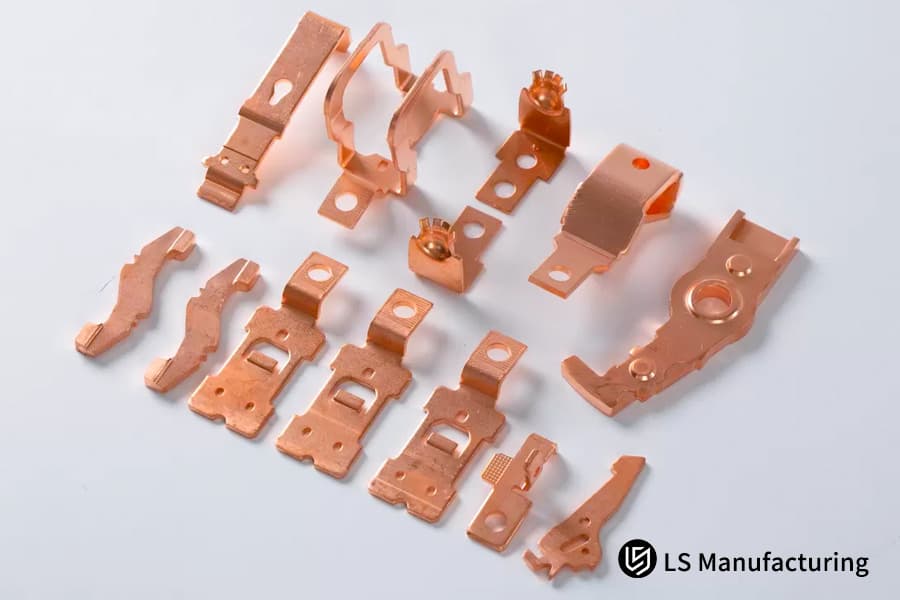
Figure 1: Various custom-stamped copper electrical contact parts with different shapes.
How To Tackle The Edge Burr Issue In Precision Copper Stamping?
The key to keeping the burr height after stamping and shearing high-conductivity copper within 0.01mm is the die single-sided clearance design and the matching of the stamping lubricating speed, which is core process standards for precision metal stamping service.
Major Reasons of Copper Burr Generation
The copper metal ductility directly influences the stamping process quality. C10200 copper exhibits the highest ductility and it can be easily work-hardened. Also, if adhesive material sticks to the punch during the high-speed stamping of this copper, hard burrs with a size of more than 0.05mm can be formed. These burrs can result in electroplated layer surface roughness and localized flow shunting that will ultimately hamper the safety of electrical contacts. Reliable metal stamping can be used to prevent manufacturing defects.
Unique Deburring Process Setting Solution
After working on high-voltage terminal stamping projects, we found out that suitable parameter ratio can thoroughly eliminate burr problem:
| Material Thickness | Die Single-Sided Clearance (Material Thickness Ratio) | Stamping Oil Viscosity | Punch Coating Type | Target Burr Height |
| 1.0mm | 6.8% | 20 cSt | TD Coating | ≤0.008mm |
| 1.5mm | 7.2% | 22 cSt | TD Coating | ≤0.010mm |
| 2.0mm | 7.5% | 25 cSt | DLC Nano Coating | ≤0.012mm |
This solution can strictly control contact burrs to within 0.01mm, meeting the burr-free requirements of automotive grade custom electrical contact stamping. To obtain the complete process parameter table, you can receive a free customized deburring process solution.
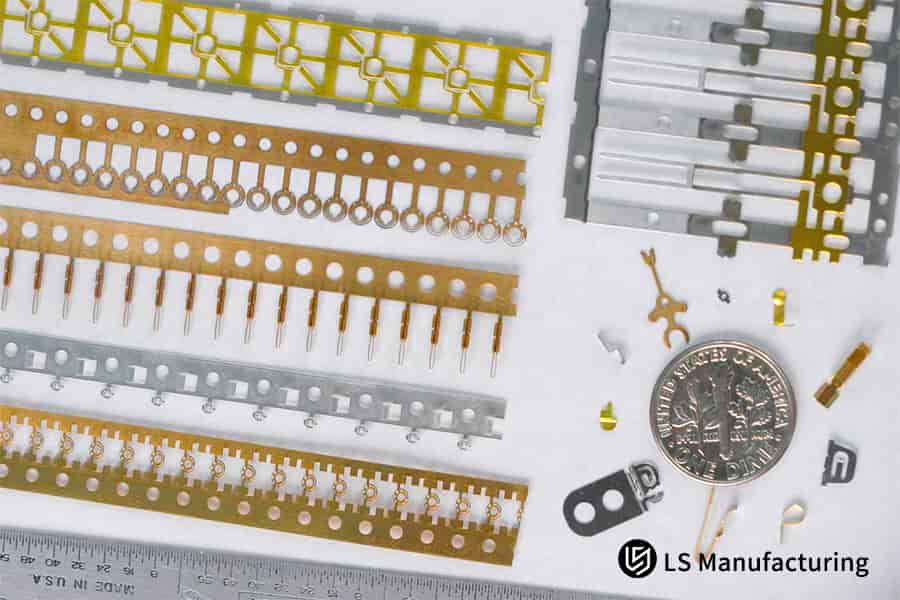
Figure 2: Precision-stamped copper contacts and machining debris on a surface.
What Are The Best Solutions For Springback Control In Brass Stamping?
The underlying solution to solve the problem of excessive bending and rebound of brass electrical contacts is to use over bending compensation molds and fine micrometer level pressure finishing at the bottom dead center, with the core achieving precise landing of springback control in brass stamping.
Major Point of Brass Springback Inaccuracy
Variability of brass hardness stands as something important in bending precision. Brass types C26800 and C2600 are known to have high work hardening indices, so that the springback angles often change erratically from 2.5° to 4.5° after bending. Due to material hardness variations from one batch to another (HV95-115), the coaxiality and sealing of a contact assembly can be severely affected. Only reliable metal stamping machining can compensate for these batch-to-batch differences in precision.
Micron Level Springback Control Technology
- Intelligent Over-bending Compensation: The die has a feedback block of elastic modulus built in, so it presets a 3.8° over-bending compensation to offset the natural springback of the material.
- Final Precision Adjustment: A pressure rib station is provided in the progressive die to deliver the unit correction force of 150MPa that will break the disordered crystal structure and, at the same time, remove residual stresses in the material.
- standard Parameter Selection: Having the bending radius equal to the material thickness and the yield strength allows the angle tolerance of a 90° bend to be stably controlled within 0.5°.
Which Clamping Solutions For Brass Avoid Microcracking Under Acute Bending?
To prevent microcracking of high-hardness brass contacts at acute bends less than 1.0T, it is necessary to strictly standardize the layout of texture angles and carry out progressive forming, which are the key technologies of reliable stamping solutions for brass.
Core causes of microcracking
Deviating the grain direction leads to cracks along bends. Most manufacturers do not give grain direction of brass rolling much thought. If they misalign the bending line with the grain elongation direction, microcracking (around 20μm-40μm) will occur. Vibrational operation over time will lead to fatigue fracture, shortening the product's life much. High speed metal stamping operation needs a dedicated forming process to prevent cracks from appearing.
Zero-crack stamping forming standards
We learned through our practical experience in the mass production project of phosphor bronze contacts that a dedicated forming standard can completely eliminate crack defects:
- Standardizing the layout design: It is mandatory that the bending line of the part keeps a 45 or 90 angle with the grain direction of the material to avoid stress concentration areas.
- Progressive forming process: By adopting a step-by-step forming process of R1.2 pre-bending + R0.5 precision bending, this method prevents the material's crystal lattice from being torn in a single high-intensity bend.
- Accurate parameter matching: By using forming limit diagrams to adjust parameters, zero-crack forming is achieved in the bending zone while the material's high hardness of HV120+ is kept, because of this the quality of precision stamped products is consistently ensured.
This technology guarantees the fatigue resistance of custom stamped electrical components, making them fit even for harsh industrial operating environments.
Why Are Inline Multi-Station Progressive Dies Critical For Consistency?
The only way to guarantee very tight tolerances of 0.005mm over hundreds of thousands of contacts is through the application of built-in high-precision multi-station progressive dies and infrared strip sensors, which directly determine the quality consistency of mass-produced copper stamping electrical contacts.
Major Disadvantages of Single-Station Die Mass Production
Single-station dies introduce error accumulation. The repeated clamping of single-station dies leads to cumulative positioning errors, which are the biggest reason for dimensional drift and inconsistent quality in precision contacts, this way not meeting the demands of large-scale mass production. Reliable metal stamping prototyping is aligned with mass production of different precision contacts.
Multi-Station Progressive Die Quality Assurance System
Our machinery line strictly meets the requirements of SAE J1940:2020 Precision Stamping Mass Production Standard, with excellent core configuration advantages, holistically ensuring the stability of precision stamping production:
- Multi-station integrated layout: Consolidating 18 forming stations, the entire process of feeding punching bending, and cutting is done in one stop, this way avoiding multiple clamping errors.
- Superior positioning mechanism: The servo feeder delivers a stepping precision of 0.002mm, combined with a double-locking position by an in-mold side-edge guide pin.
- Continuous online examination: The CCD vision system records 100% of the geometric tolerances. Automatically either compensation is done or the machine is stopped if three successive pieces are found beyond the 3 limit, enforcing absolute quality control.
This precision metal stamping service system can achieve zero-tolerance drift for millions of products. To secure a stable mass production solution for the same product, submit your drawings to receive a customized mass production quote.
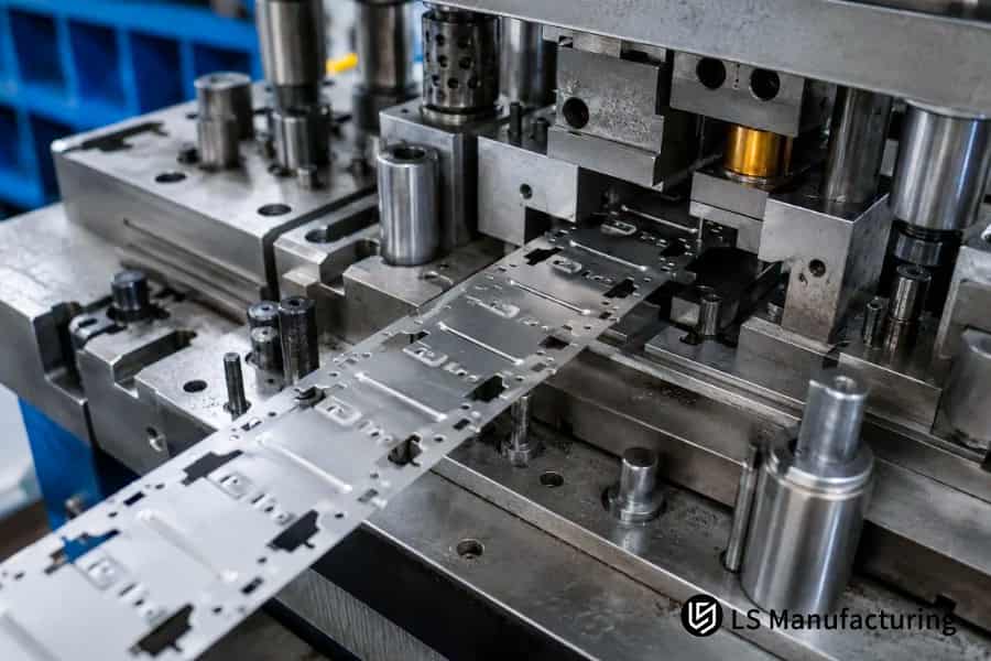
Figure 3: A progressive die stamping machine pressing a metal strip with multiple punches.
How Can Custom Electrical Contact Stamping Prevent Rapid Tool Wear?
The sector's planned approach to counter the problem of pure copper adhesion and high wear of high-speed stamping cutting edges is to employ powdered high-speed steel with ultra-fine tungsten steel inserts, which will guarantee the stability of custom electrical contact stamping mass production from the mold material standpoint.
Fundamental Reason for Mold Wear
Copper cold welding is the cause of tool wear. Due to the really high ductility of pure copper, cold solder adhesion may easily happen, which means punch edge peeling and gap collapse, causing ultimately dimensional drift in batch products. Not only does frequent downtime for mold repairing cause serious delays in delivery but also it leads to the raise of costs.
Mold Wear Resistance Strengthening
- High-end Material Replacement: ASP-23 powder high-speed steel (HRC62-64) and KG7 ultrafine tungsten steel are used to upgrade the hardness of the base metal instead of the traditional Cr12MoV steel.
- Nano-coating Enhancement: Titanium carbon nitride films can be 10-20 times harder than ordinary steels and bear very little friction with the sliding partner. A 2.0μm thick DLC diamondlike carbon coating drops the surface friction coefficient under 0.1, which means that the occurrence of copper adhesion is prevented, and the effective extension of the mold life is achieved.
- Mold Repair Cycle Renewal: The stamping operations performed from one mold repair are increased from 50,000 to 350,000. This change has an impact on downtime losses and production costs, reducing them drastically.
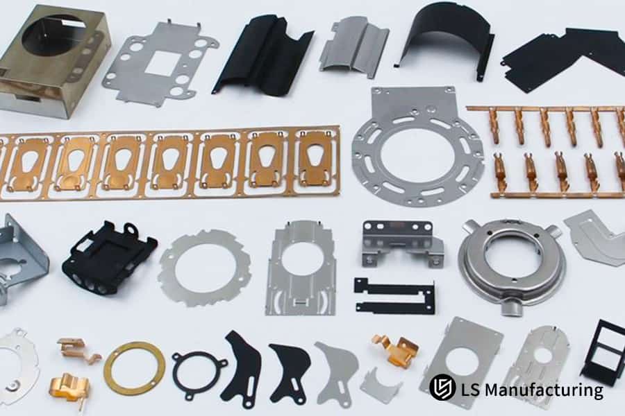
Figure 4: An assortment of brass stamped components for electrical contacts on white.
Does Your Custom Metal Stamping Service Guarantee Zero Plating Delamination?
The technical method that can be used in removing blistering and peeling of the electroplated layer on the surface of electrical contacts after stamping is by doing a thorough degreasing process and also by controlling the nano-level nickel underlay layer. This way, a very robust quality defense line can be built for the surface treatment of your custom metal stamping service.
Main Problem of Plating Delamination
Residual oil contamination adversely affects the quality of the plating. Residual lubricating oil hydrocarbons from stamping can be trapped in the inaccessible areas of bending parts and it can bring blistering, peeling and the plating getting oxidized during high temperature welding which results in total failure. Without the right surface treatment, the stamping product cannot be up to standard.
Complete Plating protection Technology Through Process
- Thorough degreasing and cleaning: This is done by using 18 megohm ultrapure water five-stage ultrasonic cleaning, 100% removal of microscopic oil residue is ensured because of this the stable performance of the subsequent electroplating processes is secured.
- Regularized underlay plating: It is necessary to apply a nickel sulfamate underlay layer of 2.5-3.5μm thickness which will act as a stable base for surface silver and tin plating.
- Accuracy thickness check: Using XRF thickness gauges complete point sampling inspection is done to ascertain that finished products will pass a 24-hour neutral salt spray test which is the corrosion protection requirement of high-end connectors.
How Can Premature DFM evaluation Reduce Custom Stamping Quote Prices?
Embedding Deep Manufacturability (DFM) measures at the prototype design phase can enable R&D teams to remove about 92% of potential injection molding faults even at the stage of mold opening. They can also witness a 30% direct reduction of mass production amortization quotes, so effectively managing the mass production cost of custom stamped electrical components.
Cost Downside of Traditional Processing Modes
Going through a blind trial production route escalates overall costs. Ordinary stamping manufacturers blindly follow the drawings for sampling, ignoring the issues of forming stress and material loss. During the mass production stage, they frequently repair molds, resulting in skyrocketing unit costs and delayed delivery times. Economic metal stamping optimization can control mass production costs from the source.
Essence of DFM Pre-Production Optimization
The only cost calculation method: Stamping Mass Production Unit Cost = Die Amortization Cost Total Capacity + Material Loss Cost + Processing Cost. A well thought out pre-production can be very effective in cutting down various expenses.
- Defects Simulation Forecasting: In one day maximum, AutoFORM 3D CAE simulation helps find a range of issues such as springback and excessive thinning rate and in this way, mass production risks are minimized.
- Enhanced Efficiency in Material Usage: Decreasing the sample spacing from 3.0mm to 1.8mm gives a substantial reduction in the amount of scrap.
- Trial Molding Expenses Lowers: Keeping the trial molding to the minimum of 2 (or less), samples are delivered rapidly within 14 days even when certified, the die amortization cost is lowered.
Pre-production DFM optimization allows stamping solutions for brass to have both quality and price advantages. Want to proactively avoid mass production risks? Get a free professional DFM assessment report.
LS Manufacturing Custom Brass Stamping for Electric Vehicle Busbars
The large-scale production of high-voltage brass contacts for new energy vehicles is often hindered by problems like springback variations and welded joint failures. Capitalizing on their mature springback control in brass stamping, LS Manufacturing has managed to solve a mass production crisis in the international automakers' supply chain.
Client Problem
In November 2025, a top German Tier 1 automotive parts manufacturer suffered a major shut down in the mass production of C26800 brass compound contacts for an 800V new high-voltage fast charging system. Its current European vendor failed to fix the 4.2° residual springback problem in the high-speed stamping process, leading to a 0.15mm deviation in the contacting surface.
Such a defect resulted in incomplete welding and spattering issues with the automated laser welding, leaving only a 74% yield of the product. Apart from causing the delay of the whole vehicle mass production plan, the customer was also exposed to expensive supply chain claims emphasizing the crucial role of precision stamping process control.
LS Manufacturing Solutions
Responding to the customer's call for help, LS Manufacturing immediately organized a task force of five highly experienced mold engineers. Initially, we took samples for rechecking the mechanical properties of the raw materials and determining the accurate hardening curve. Afterwards, the group went the extra mile and constructed a 16-station ultra-high-speed progressive die system capable of reaching a maximum stamping speed of 320 spps (strokes per minute), including a three-stage bending springback compensation procedure.
At the same time, a super-hard KG7 tungsten steel punch HV2800 was utilized applying a 180MPa instantaneous pulse pressure at the point of bending to loose the internal stress. This, together with employing an online laser rangefinder for real-time closed-loop adjustment of the press's bottom dead center stroke, thoroughly guaranteed the stamping forming accuracy.
Results and Value
These enhancements were very substantial. Batch flatness of the custom electrical contact stamping products was controlled at the level of 0.04mm, which was way better than the client's drawing standard of 0.08mm. The product's capability index CpK was 1.67, microcrack detection during bending was 0%, and the laser welding yield went up to 99.95%. Thanks to this optimization, the customer was able to cut the unit production cost by 28%, shorten the delivery time by 4 weeks, and eliminate completely the supply chain bottlenecks, which led to receiving a high level of recognition from overseas clients.
This case fully demonstrates the empowering value of precision stamping technology for high-end mass production projects. Do you face similar high-pressure contact mass production challenges? You can consult LS Manufacturing engineers one-on-one to customize a dedicated solution.

FAQs
Q1: What is the standard dimensional tolerance of your precision metal stamping service for electrical components?
Our trust is in high-precision fully servo progressive die equipment, together with an in-die vision compensation system to ensure the critical dimensional and positional tolerances of electrical contacts in large-volume continuous stamping to be within 0.005mm, which is the standard for automotive-grade mass productions.
Q2: How does LS Manufacturing ensure consistent springback control in brass stamping across different raw material batches?
Sampling tests are made on the yield strength and hardness of each batch of brass coils, and the differences in material parameters are recorded. By the very subtle adjustment of the die bottom dead center finishing pressure at the micron level, springback differences of various batches can be negated.
Q3: Can you quote a competitive individual price for custom-stamped electrical components with a low MOQ?
We are able to provide customized supply chain solutions which could include division of process costs and die amortization costs for small-batch prototyping, trial production, and mass production, offering detailed and market-based transparent pricing information that matches low MOQ requirements. You can also upload your drawings directly for a quick and accurate mass production quote.
Q4: Why is LS Manufacturing the leading copper stamping electrical contacts supplier in China?
Our deep industry involvement for 20 years has given us a profound understanding of copper and brass mold development. All of our machinery is installed with in-mold infrared dimension sensors, allowing for quality control in real-time at every stage of production, resulting in a good balance of precision, stability, and delivery efficiency.
Q5: How do you solve the edge burr problems inherent in premium copper and brass stamping services?
The first step is to fix the one-sided clearance of the mold cutting edge to the best value of 7.2% of the thickness of the material. Coupled with the use of TD-coated high-speed wear-resistant punching tools and a special lubrication method, we are able to consistently keep the burr level at the contact point within 0.01mm.
Q6: Would your custom metal stamping be able to provide complete surface plating on the components, like silver or nickel plating?
Besides the production services, we also offer product finishing and delivery services. Our silver and nickel selective plating processes are high-precision, fully automated, and one-stop. The uniformity of the plating is great, and all the products that come out of the line are capable of reliably enduring a 24-hour neutral salt spray corrosion test.
Q7: What technical data or documentation does your factory provide before starting custom electrical contact stamping production?
Before the official mold opening, we will provide the customer with a complete DFM manufacturability optimization report, and synchronously provide stress and deformation dynamic data simulated by automatic spreadsheet software to avoid all molding defects in advance.
Q8: How long does LS Manufacturing take to deliver verified tool samples for complex stamping solutions for brass?
Based on the use of advanced CAE digital simulation technology and adaptable mold repair techniques, we are able to drastically reduce the time it takes for trial molding, so we can guarantee that the customers complex brass stamping samples that have been fully inspected and are qualified will be shipped to them within 14 working days.
Summary
Mass production of high-quality copper and brass electrical contacts These days is, at its very root, the deep integration of various technologies and knowledge. It is not limited to the control of materials properties but also covers design precision and mold stress, surface treatment, and much more. Small burrs, springback errors, and microscopic cracks can cause safety hazards that are on a drastically different scale, like equipment leakage, thermal runaway, and welding failure.
LS Manufacturing directs its efforts towards technical parameters supported by numbers, quality control systems that are standardized, and studies based on actual cases. By taking advantage of SPC/CPK mass production control and micron-level mold optimization technology, it thoroughly addresses the issue of consistency in the mass production of precision electrical contacts and guarantees the safe and steady operation of new energy and smart grid equipment.
CUT the R&D and supply chain costs that come from quality deviations and delivery delays in low-end processing! If you are currently in the phase of drawing development or mass production replacement for high-voltage busbars, circuit breaker terminals, or precision copper springs, you can send 2D/3D engineering drawings anytime and get a free professional DFM technical evaluation plus a very competitive mass production quotation.
📞Tel: +86 185 6675 9667
📧Email: info@lsrpf.com
🌐Website: https://lsrpf.com/
Disclaimer
The contents of this page are for informational purposes only. LS Manufacturing services There are no representations or warranties, express or implied, as to the accuracy, completeness or validity of the information. It should not be inferred that a third-party supplier or manufacturer will provide performance parameters, geometric tolerances, specific design characteristics, material quality and type or workmanship through the LS Manufacturing network. It's the buyer's responsibility. Require parts quotation Identify specific requirements for these sections.Please contact us for more information.
LS Manufacturing Team
LS Manufacturing is an industry-leading company. Focus on custom manufacturing solutions. We have over 20 years of experience with over 5,000 customers, and we focus on high precision CNC machining, Sheet metal manufacturing, 3D printing, Injection molding. Metal stamping,and other one-stop manufacturing services.
Our factory is equipped with over 100 state-of-the-art 5-axis machining centers, ISO 9001:2015 certified. We provide fast, efficient and high-quality manufacturing solutions to customers in more than 150 countries around the world. Whether it is small volume production or large-scale customization, we can meet your needs with the fastest delivery within 24 hours. choose LS Manufacturing. This means selection efficiency, quality and professionalism.
To learn more, visit our website:www.lsrpf.com.